")
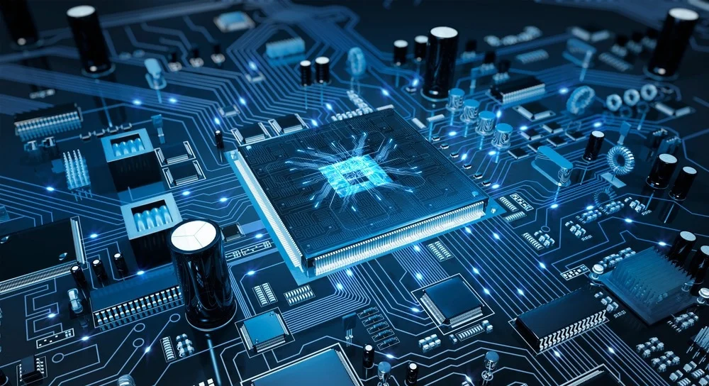
Nanoelectronics, where the semiconductor component’s key characteristics, such as logic transistors, memory and other components measure at less than 100 nm is a rapidly expanding area. The potential applications of quantum computing and advanced memory and even energy storage and generation create tiny technology possessing huge potential.
History of Nanoelectronics
The first electronic devices that were nanoscale were invented by scientists in the early 1960s. They created gold thin films only 10 nanometers thick to serve as the basis for a junction transistor.
In the 1980s, a group of IBM researchers developed the world’s first field effect transistor (MOSFET) featuring the gate oxide’s thickness of 10 nm. It was made using the tungsten gate technique to complete this nanoscale size.
One of the first three-gate MOSFET that was a multi-gate MOSFET, called the FinFET was created in 1989. The FinFET or Fin field effect transistor is a dual gate MOSFET which is three-dimensional as well as non-planar. In 2002, a 10- millimeter FinFET was manufactured.
An CMOS (complementary MOS) transistor was created in 1999, to demonstrate what MOSFET transistor technology can be able to take us on the path of Nanoscale electronic devices.
A few years later In 2006, scientists came up with an MOSFET with a size of just 3 nm which made it the tiniest ever nano-electronic device that time.
Nanoelectronic semiconductors entered commercial production in the decade of 2010 Then, Samsung is presently releasing the 3 nanometer GAAFET which is a gate all-round FET that is available on the market.

How Was Nanoelectronics Made Possible?
Nanoscale electronic devices represent the culmination or, perhaps of the most recent product from decades of leading-edge research into nanosciences and nanotechnology.
Since Richard Feynman proposed the possibility of a computer with “submicroscopic” computers in a remarkable lecture in the year 1959, scientists working who are at the cutting edge of physics, instruments, materials science and engineering and manufacturing research are pursuing ever-smaller tiny tests.
The journey led to numerous groundbreaking technologies that utilize information and communications technology (ICT) such as personal phones, computers, Internet of Things (IoT) technology and more. every day game changers in the present are based on advances in Nanoelectronic research.
- However, the nanoelectronic gadgets have yet to hit the shelves of our stores.
- The advancement of semiconductor technology is significantly, microcomputers remain largely far away. Sub-micron (nanoscale) computer systems could remain a long way off.
- Technology in semiconductors may be restricted in terms of minimal system size We could be nearing that threshold.
- Nanoelectronics that are currently in research could allow us to crack this wall through the development and production of really sub-micron, nano-scale electronic gadgets in the coming few years.
Moving Nanoelectronics Forward
Researchers suggest that researchers propose that perfect method to create nanoelectronics is by combining microelectronic devices along with nanoelectronics in hybrid devices.
This approach builds on the progress already achieved in microelectronics, for example, in developing microelectromechanical systems (MEMS) technology which has brought numerous MEMS sensors like accelerometers and microphones, magnetometers and gyroscopes, and even power generators to the market.
One of the latest innovations pursuing the hybrid method is a quantum effect nanoelectronic device that is used for resonance tunneling. It uses a conventional Silicon bulk effect transistor in order to create a multi-state switch device that its creators identify as”a “resonance tunneling transistor.”
- A resonance tunneling transistor could be employed to make circuits that have a greater density of available logic than the conventional microelectronic transistor can offer.
- A different nanoelectronic device under research could be the single-electron transistor, or the SET. It is a switch device which controls electron tunneling, and utilizes this process to improve the power of a current.
- Two tunnel junctions, comprised of two pieces metal, with a sub-nanometer thin insulation between them, have the same electrode. Electrons have to travel through the insulator in order to pass between electrodes.
- Since quantum tunneling is an isolated process that produces electric charges by electrons passing through the tunnel junction are created in large quantities of every electron’s charge.
Equipments such as electronic tunneling equipment and quantum dots operate using quantized energy. Quantized energy is energy that has the smallest possible parts that interact that are at the scale of quantum physics phenomena such as tunneling, particle entanglement and superposition of particles are visible.
Nanoelectronics devices are able to emit electrons in extremely small areas. Of course, quantification of energy and the effects it has on devices and the intended uses they serve are major research areas in the present.
The other area of focus within the field of nanoelectronics is exploring ways of using electroconductive polymers for small-scale organic electronic circuits.
Researchers are examining electricallyconductive nanostructured polymers and nanoparticle-based ones, as well as polymer nanocomposites containing Nanoparticles that conduct electricity.
They are ideal to create nanoscale electronic devices made of organic. This is because of the Nanopolymers’ capability as building blocks that can be used for simple or complex hi-level nanostructures.
Nanostructured and organic nanoelectronics systems are also able to be employed together with polymers that are p-conjugated for electron acceptors in the next generation of organic photovoltaics at nanoscales.

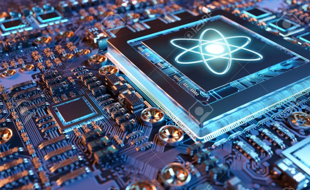
Spintronics
Apart from transistors, the nanoelectronic device are also involved in the storage of data (memory). In this case, spintronics is the research and use in solid-state electronics of electron spin as well as its associated magnetic moment along with charge electric – is a well-established technology. Find out more here: ” Graphene spintronics – from science to technology”.
It also has a part to play in the new technology that harnesses quantum behaviour to compute (read moreabout it ” Quantum computing moves forward with spintronics progress” and ” The birth of topological spintronics”).
Optoelectronics
Electronic devices that generate the light, control it and detect it as well as control light i.e. optoelectronic devices come in various shapes and designs. They are extremely energy efficient (less heating and power usage) optical communications have become increasingly significant because they offer the capability of solving one of the most pressing issues that we face in the information age the issue of energy consumption.
In the area of nanotechnology Nanofibers, such as nanoparticles (see for example: ” Light-emitting nanofibers shine the way for optoelectronic textiles”) as well as carbon nanotubes have been utilized particularly graphene, which has demonstrated amazing potential in optoelectronic circuits.
Displays
Display technologies are grouped in three major technological areas: Organic LEDs, Electronic printing as well as other equipment designed to display images in stills, as well as field Emission Displays. For more information, refer to our article on Nanotechnology for Displays.
Wearable, flexible electronics
The time of wearable electronic devices is now upon us, as shown by the rapid growth of fitness bands, as well as other new-generation devices for monitoring health like electronic tattoos.
If the current research findings are evidence that wearable electronics are coming, they will extend beyond tiny electronic devices, or wearable computers. These devices will not only be embedded within textiles, but the electronics gadget or system might eventually transform into a fabric.
Electronic fabrics (e-textiles) can enable the development and manufacture of new types of clothes that have electronically-controlled sensors that are distributed across the entire garment. E-textiles of this kind will have the ability to be revolutionary in their ability to detect the environment, perform, store as well as emit such as biomedical monitoring or the development of new man-machine interfaces and, in the excellent case scenario, leverage an existing textile manufacturing system that is low-cost (see for example ” wearing single-walled carbon nanotube electronics on your skin” as well as the ” temporary tattoo to monitor glucose levels” or ” graphene nanosensor tattoo on teeth monitors bacteria in your mouth”).

Nanoelectronics in Energy
Supercapacitors and solar cells are two examples of the areas in which nanoelectronics plays a significant function in energy generation as well as storage. For more information, read the sections that we have written about Nanotechnology within Energy as well as Graphene Nanotechnology for Energy.
Molecular Electronics
In contrast to nanoelectronics, in which devices are scaled to nanoscale scales molecular electronics is concerned with electronic functions that are found within molecular structures, such as the ones found in nature, including photosynthesis and signal transduction.
The goal of Molecular Electronics is to develop the foundational understanding of charge transportation via molecules. It is fueled by the desire to create molecular circuits as a way to build tiny high-performance and energy efficient computer systems (see for example: ” Adding an optoelectronic component to molecular electronics”).
Electronic materials can be used to create applications.
Nanoparticles may be utilized as dielectric materials, conductive substances and piezoelectric substances since they’re easy to charge electrons and then escape them. Nanoscience and technology the field of nanoelectronics and technology forms the foundation of the field of nanoscience and technology. Nanoelectronics and science is an inevitable extension from the progress of microelectronics. However this is an entirely novel field in which it is possible to build quantum structures, quantum devices quantum circuits, as well as quantum systems that are based on concepts of new ideas.
- Nanoelectronics may break the boundaries of conventional technology, and exploit the structure and information capabilities of materials, dramatically increase the capability of processing and storing data per volume of material. It can also actually achieve groundbreaking advancements in the collection of information and processing capabilities.
- Due to the crucial importance of nanoelectronics within the realm of information technology, United States, the European Union, Germany, and Japan are drafting the strategy for development that includes Nano Electronics Technology and deployed initiatives. At the close of the 20th century the nanoelectronics field was carried out in China as well as in Japan. Nanoelectronics has been recognized as the main area of research and development in the nanoscience and technology field for a number of years.
- Influenced by the policy of different nations, nanoelectronics has grown rapid in all parts of the world in the last decade. Recently, silylene, black-phosphorus hexagonal boron Nitride, transition metal salts and monolayer molybdenum disulfide have been one of the main trends within the field of material research for nanoelectronics. Furthermore, in comparison to metals, oxides, and crystals the study in semiconductors has also grown significantly.
- Gallium arsenide as well as silicon are two types of semiconductors with more study. Gallium arsenide research continues to grow, while the research into silicon has slowed although the exact proportional decrease isn’t clear. Research on graphene as well as boron nitride and molybdenum disulfide have been boosted. But, when compared to carbon nanotubes, silicon nanowires semiconductor nanowires, as well as others with a decrease in the amount of research articles, graphene nanobelts as well as epitaxial graphene show a greater increase in the quantity of research articles.
- Nanomaterials are used extensively and are advancing in electronic applications. Zhang et al . [66] suggested different strategies for the preparation for flexible electronic devices that are built on LM nanoink. It is a broad field of application for printed electronic devices. The LM nanoink regulates stability and biocompatibility, and offers the potential to be a key component in future implementation of devices with flexible electronics.
- Nanopowders and particle are extensively employed in the field of nanoelectronics science and technology including nanoelectronic devices that are paired with microelectronics are hot. From the early 20th century, technology based on nanoelectronics has had an enormous influence on our lives and our work.
In accordance with Moore law, the size of integrated circuits (IC) is growing by 4 times per 3 years. The dimensions have been shrinking for the past 30 years. The size of electronic devices continues to decrease as well, the demands for integration of integrated circuits are getting more and more demanding. The question of finding ways to create more cost-effective and energy-efficient semiconductor chips is an important issue for all to understand.
In order to make smaller electronic devices more reliable It is the current trend to incorporate nanotechnology in electronic gadgets. Nanoscale electronic devices can be reduced further as well as the performance of these devices will closely correlated with quantum properties of device.
With the addition of graphene nanoparticles to the cooling system as well as the cooling system, Babith Lawrance and Renish have significantly increased the efficiency of convective heat transfer of water. This results in a significant cooling effect when compared to the standard cooling method [67]. Quantum nanoelectronic devices are equipped to actually achieve greater functions that are related to altering the frequency of the electron wave. They also are more efficient and have lower usage in order that it can address the issue of consuming energy.
Optoelectronic technology today has gradually progressed to new nanooptoelectronic technologies, and the development of nanooptoelectronics has been incorporated during the advancement of conventional semiconductors, and has, ultimately, has emerged as a revolutionary technology that will be the next step in the evolution of nanoelectronics that are emerging.
- Nanotechnology may benefit to understand the relationship between photons and electrons in every nanostructure. In the end, photoelectrons and nanoelectronics technology is merged. A new kind of technology and science, nanooptoelectronics is a result of the fusion of engineering and science as well as the result of constant advancement based on technology that is currently in use.
- In the same way being a result of the combination of electronics and nanotechnology the nanooptoelectronic technologies will eventually enable humans to control a one atom at desires. Traditional nanooptoelectronic devices typically include electronic devices as well as nanoelectronics.
- Nanoelectronic devices are comprised of nanophotoelectric detectors, nanoluminescent devices display devices, nanodisplays and more. Nanophotoelectric technology detectors are typically comprised of nanowires as well as various kinds of nanorods, or nanopowder that is coated. Infrared detector is one of the most popular device that uses nanophotoelectric technology and is highly sensitive when used.
With the advent of nanooptoelectronics, nanolight and other materials that are fundamental, most advanced nanolight emitting devices are being constructed. From a structural point from a structural perspective, we could make use of different types of material like nanoparticles for an illuminating silicon diode. Then, we can use a variety of dimensions to produce a variety of diode that emits light. Additionally, research into the field of nanodisplay is technologically advanced.
- The most commonly utilized nanodisplay is comprised of a majority of nanotube displays and carbon nanogeneration displays. This new technology could energetically boost the power of computing of a computer, and can even decrease the speed of computing on the system in just a relatively short period of.
- The power of computer used is just one millionth that currently available computers. Nanooptoelectronics will often rise the capacity of communications by hundreds of times.
- Nanoelectronics technology is itself a technology that has great potential, and an extremely wide variety of uses. Nanoelectronic technology is advancing,
- that combines nanotechnology and new electronic components, it will be able to expand their market. It also sets more requirements for the creation of electronic components that are emerging and is gradually advancing on the process of developing them into practical products.
The development of single electron devices nanofield-effect transistors molecular electronic devices and various other innovative information devices are constantly evolving as a result of this research.
Conclusions
The field of nanoelectronics is rapidly growing which includes the creation of nanosensors with nano-sized sizes for use “from home to field.” Nanoelectronic nanodevices will be crucial to the development of analysis of high-performance. Researchers are currently working on sensors that can be carried around to use for “bed-side analyses” and “point-of-care.”
The portable sensor is regarded to be good if it’s simple to operate that it displays in real time and has the ability to measure accurately. Some nano-sized gadgets that are already commercially available as a result of nanoelectronics. Future advances in nanoelectronics could result in a number of sensors appropriate for various uses.